|
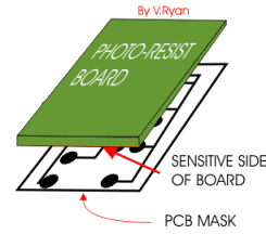
The PCB mask (now on a transparency) is placed underneath
the photo-resist board, touching the sensitive surface. Remember the plastic
film must be removed.
|
|
|
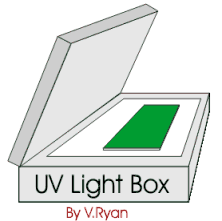
PCB mask and board are then transferred to the UV light
Box. |
|
|
The lid is shut and the box switched on. The photo-resist board, with PCB mask are left underneath the lid for 2 ½ minutes. |
|
|
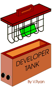
The photo-resist board is then placed in a tank filled
with developer. |
|
|
|
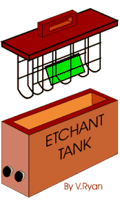
When the board is taken out of the developer it must be washed in clean water before transferring to the etching tank. Always use plastic tongs - never use your hands. The etchant is held in a ‘bubble etch tank’ and is heated. This solution slowly etches away the unwanted copper, leaving the tracks only. At this stage it is important to keep checking that the PCB is completed (time - 15 to 45 minutes). If it is left in the tank too long the copper tracks will also be removed or damaged. |