| CLICK HERE FOR INDEX PAGE | |
| THE 4081B CIRCUIT DESIGN | |
| V. Ryan © 2003-2022 | |
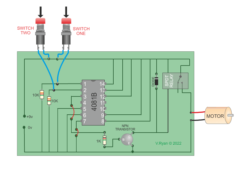
| A circuit based around the 4081B integrated circuit can be seen below. The integrated circuit (IC) contains a number of AND gates, although for this sample circuit only one of the AND gates has been used. | |
 |
|
| The circuit above represents an AND GATE. This means
that switch one AND switch two must be pressed before the relay is
energised. When logic chips are used in a circuit the inputs of any
unused gates should be connected to the positive or negative, it does
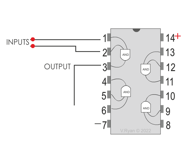
not matter which. The ‘chip’ diagram below shows the gates of the 4081B and its inputs and outputs. In the circuit above only input pins 1 and 2 are used, for the switches, which when pressed produce an output at pin 3. The output at pin 3 energises the relay and starts the motor, releasing the food for the dog. |
|
 |
|
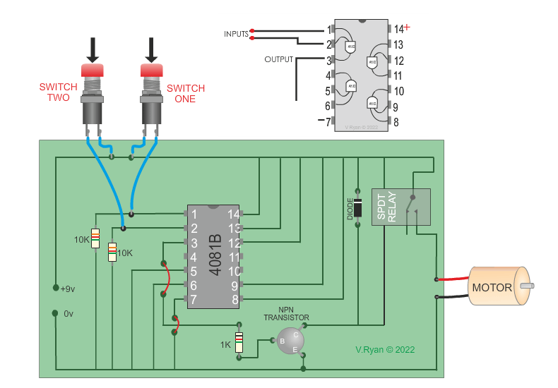
| The circuit diagram below shows the circuit operating. The 4018B animation has been added to help in understanding how the combination of the 'logic' integrated chip and other components work together. | |
 |
|
| PICTORIAL REPRESENTATION OF THE LOGIC CIRCUIT. | |
 |
|
|
QUESTIONS: 1.
How many switches can be connected to the 4081B ? |
|
|
CLICK HERE FOR MORE INFORMATION REGARDING THE 4081B LOGIC CHIP |
|
|
|
|